Description #
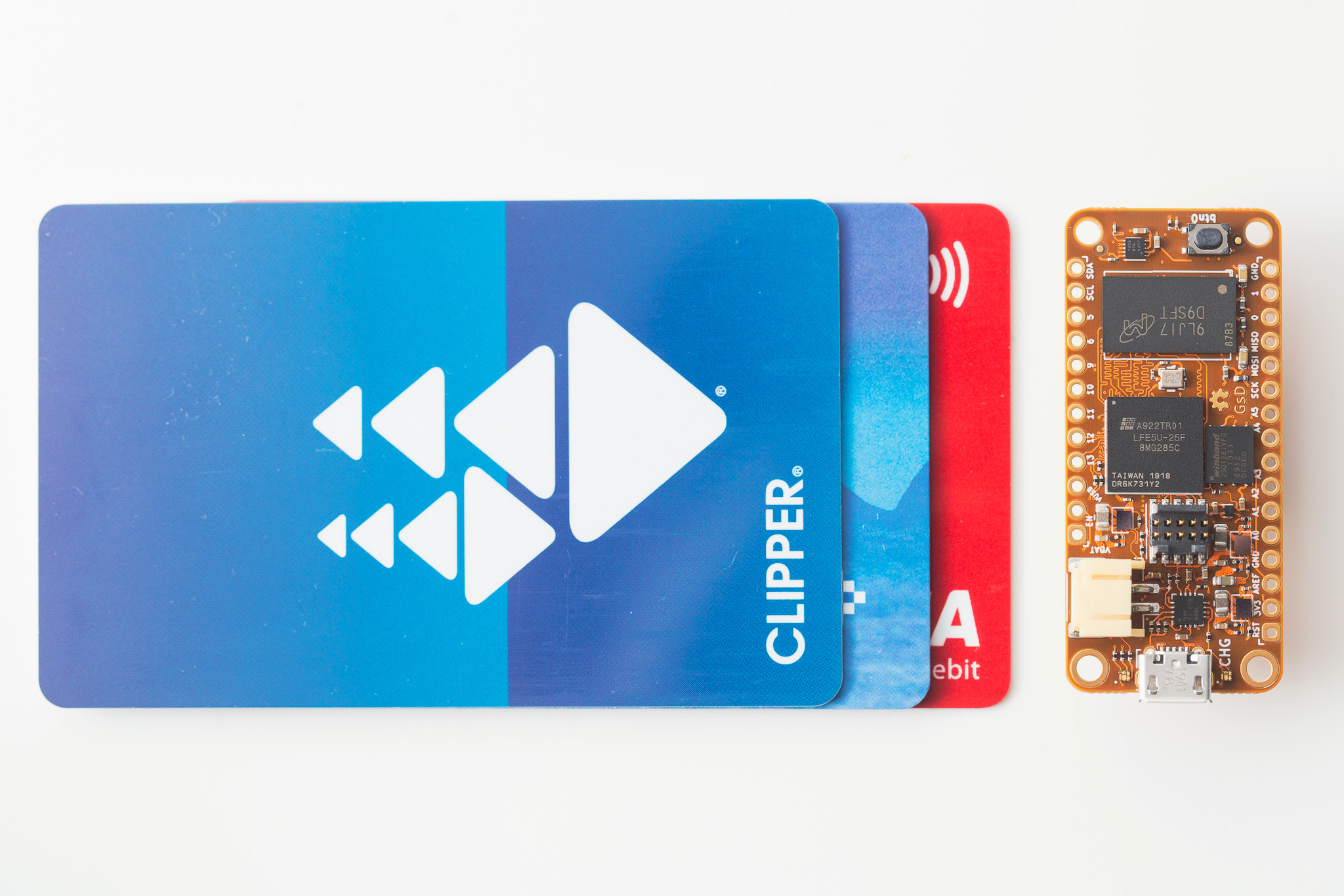
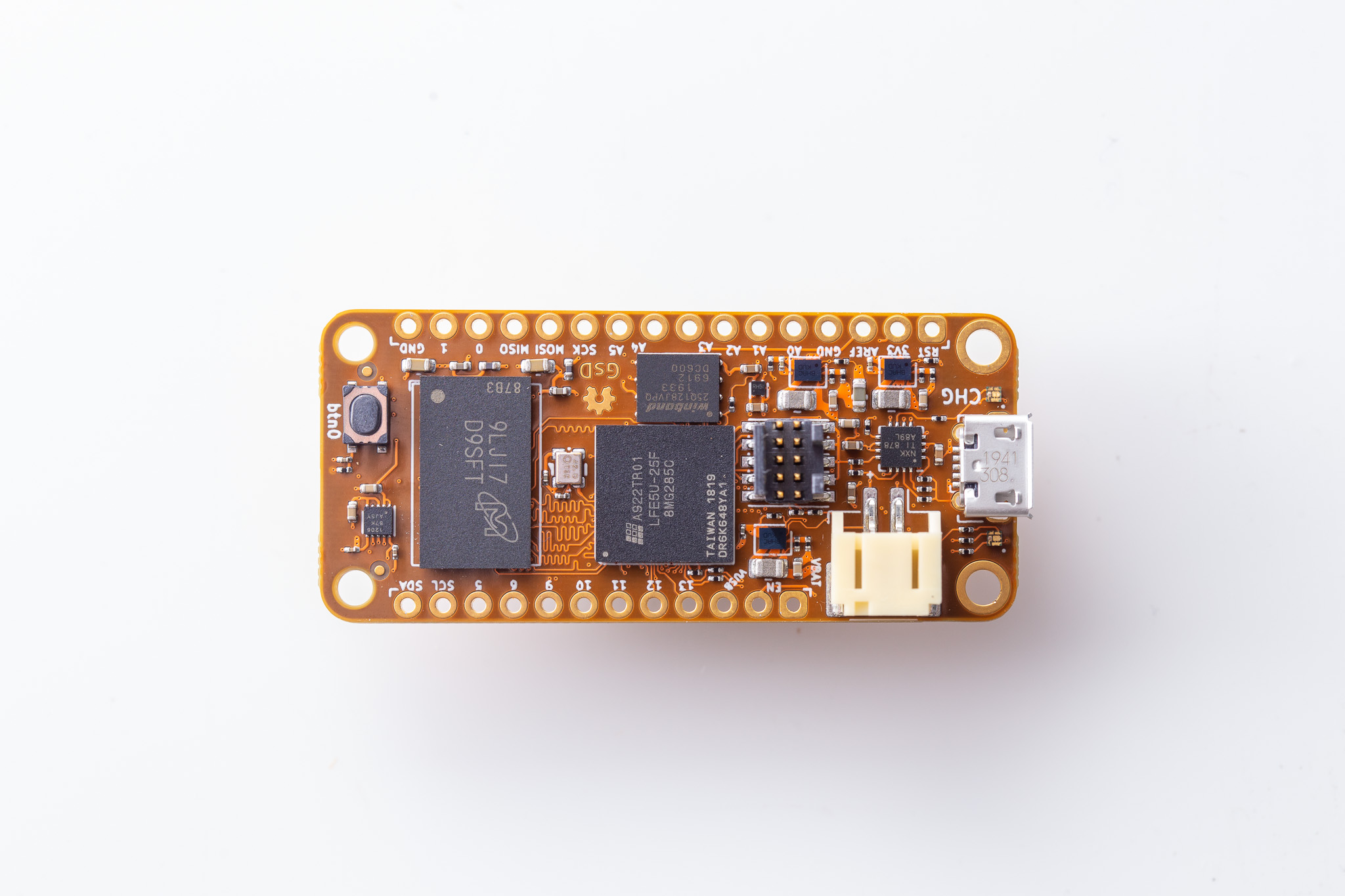
Updated version of the OrangeCrab, an electronics development board featuring a Lattice ECP5 FPGA, and DDR3 memory. Primarily designed to prototype RISCV SoC and evaluate custom peripherals.
This updated version improved the multiboot experience by connecting an FPGA I/O to the reset line.
This version was produced as a small batch for a GroupGets campaign.
Technical details #
Here are the main details for the OrangeCrab (25F)
- Lattice ECP5-25F FPGA in csfBGA285 package
- 24 K - Look Up Tables
- 1008 Kb - Embedded Block RAM
- 194 Kb - Distributed RAM
- 28 - 18x18 Multipliers
- PLLs: 2
- Internal oscillator
- Flexible I/O for DDR3 Memory Support
- DDR3L Memory
- 128 Mbytes (1Gbit)
- 64M x16
- 1.35V low voltage operation
- Micro USB connection
- Full-speed (12Mbit) USB with direct connection to FPGA
- Non-volatile Storage
- 128Mbit QSPI FLASH Memory
- Bootloader (First 4Mbits)
- User Bitstream
- User storage (Firmware/MSC backend/etc)
- QSPI compatible
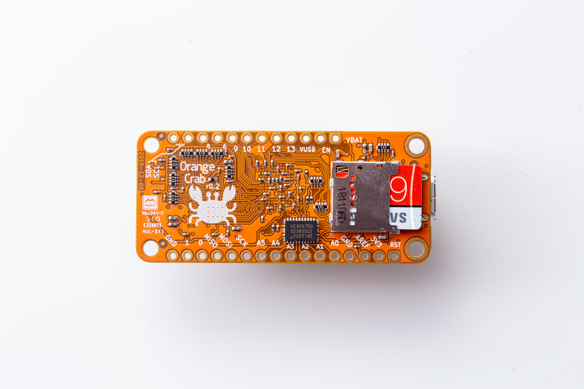
- MicroSD socket
- 4bit SD interface (CK, CMD, DAT0-3)
- 128Mbit QSPI FLASH Memory
- Power supply
- High effeciency DCDC for main supplies
- Battery charger (100mA), with charge indicator LED
- LiPo battery connector (PH type)
- 48MHz onboard oscillator
- Standard 0.05" JTAG connector
- User I/O
- 1x Button
- 1x RGB LED
- 20x I/O on 0.1" headers
- Analog System
- Analog Mux
- SAR ADC, external RC / input comparator of FPGA
- Digital bypass
- Internal channels for supply monitor
- Battery voltage sensing
- Feather Format Board
- Dimensions: 22.86mm x 50.8mm (0.9" x 2.0")
Pinouts #
DDR3 (IOVCC=1.35V) #
| Name | Pad |
|---|---|
| ADDR[0] | C4 |
| ADDR[1] | D2 |
| ADDR[2] | D3 |
| ADDR[3] | A3 |
| ADDR[4] | A4 |
| ADDR[5] | D4 |
| ADDR[6] | C3 |
| ADDR[7] | B2 |
| ADDR[8] | B1 |
| ADDR[9] | D1 |
| ADDR[10] | A7 |
| ADDR[11] | C2 |
| ADDR[12] | B6 |
| ADDR[13] | C1 |
| ADDR[14] | A2 |
| ADDR[15] | C7 |
| ODT | C13 |
| RESETn | L18 |
| Name | Pad |
|---|---|
| BA[0] | D6 |
| BA[1] | B7 |
| BA[2] | A6 |
| RAS | C12 |
| CAS | D13 |
| WEn | B12 |
| CSn | A12 |
| DM[0] | D16 |
| DM[1] | G16 |
| DQ[0] | C17 |
| DQ[1] | D15 |
| DQ[2] | B17 |
| DQ[3] | C16 |
| DQ[4] | A15 |
| DQ[5] | B13 |
| DQ[6] | A17 |
| DQ[7] | A13 |
| DQ[8] | F17 |
| Name | Pad |
|---|---|
| DQ[9] | F16 |
| DQ[10] | G15 |
| DQ[11] | F15 |
| DQ[12] | J16 |
| DQ[13] | C18 |
| DQ[14] | H16 |
| DQ[15] | F18 |
| DQS_n[0] | B15 |
| DQS_p[1] | G18 |
| CLK_p | J18 |
| CKE | D18 |
| *virtual_vccio[0] | K16 |
| *virtual_vccio[1] | D17 |
| *virtual_vccio[2] | K15 |
| *virtual_vccio[3] | K17 |
| *virtual_vccio[4] | B18 |
| *virtual_vccio[5] | C6 |
| *virtual_gnd[0] | L15 |
| *virtual_gnd[1] | L16 |
- Virtual VCCIO and GND are connected to VCCIO and GND on the PCB. They should be driven HIGH and LOW respectively to reduce SSO noise on the DDR3 I/O bank.
General (IOVCC=3.3V) #
| Name | Pad |
|---|---|
| GPIO0 | N17 |
| GPIO1 | M18 |
| GPIO5 | B10 |
| GPIO6 | B9 |
| GPIO9 | C8 |
| GPIO10 | B8 |
| GPIO11 | A8 |
| GPIO12 | H2 |
| GPIO13 | J2 |
| GPIOA0 | L4 |
| GPIOA1 | N3 |
| GPIOA2 | N4 |
| GPIOA3 | H4 |
| Name | Pad |
|---|---|
| clk48 | A9 |
| rgb_led0_r | K4 |
| rgb_led0_g | M3 |
| rgb_led0_b | J3 |
| BTN | J17 |
| RSTn | V17 |
| USB_p | N1 |
| USB_n | M2 |
| USB_pu | N2 |
| QSPI_CSn | U17 |
| QSPI_CLK | U16 |
| QSPI_DQ[0] | U18 |
| QSPI_DQ[1] | T18 |
| QSPI_DQ[2] | R18 |
| QSPI_DQ[3] | N18 |
| Name | Pad |
|---|---|
| SD_DAT[0] | J1 |
| SD_DAT[1] | K3 |
| SD_DAT[2] | L3 |
| SD_DAT[3] | M1 |
| SD_CMD | K2 |
| SD_CLK | K1 |
| SD_CD | L1 |
| ANA_MUX[0] | F4 |
| ANA_MUX[0] | F3 |
| ANA_MUX[0] | F2 |
| ANA_MUX[0] | H1 |
| ANA_SENSE_L | G3 |
| ANA_SENSE_H | H3 |
| ANA_CTRL[0] | G1 |
| ANA_CTRL[1] | F1 |
Photos #

